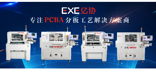
Troubleshooting Common PCB Depaneling Machine Issues: Edge Chipping, Component Damage, and Alignment Errors
PCB depaneling—the process of separating individual PCBs (or “panels”) from a larger production panel—is a critical final step in PCB manufacturing. Even minor flaws in depaneling (e.g., chipped edges, damaged components) can render boards non-functional, leading to scrap rates, rework costs, and delayed deliveries. Among the most frequent issues plaguing depaneling operations are edge chipping, component damage, and alignment errors—each tied to machine setup, tooling, material properties, or process parameters.
This article breaks down the root causes of these three core issues, provides step-by-step troubleshooting workflows, and shares preventive measures to ensure consistent, high-quality depaneling for both rigid and flexible PCBs (FPCs).
I. Edge Chipping: Causes, Troubleshooting, and Prevention
Edge chipping—small cracks, missing copper, or substrate damage along the cut edge of a PCB—compromises mechanical integrity and can expose internal layers to moisture or contaminants. It is most common with brittle substrates (e.g., FR-4, high-frequency laminates like Rogers) and aggressive cutting methods (e.g., mechanical routing, punching).
1. Root Causes of Edge Chipping
Edge chipping occurs when the cutting force or tool interaction exceeds the substrate’s tensile strength, or when the cut path is poorly optimized. Key causes include:
Dull or worn cutting tools: Blunt router bits, V-cutters, or laser lenses cannot cleanly shear the substrate, leading to tearing instead of a smooth cut.
Excessive cutting speed/force: High feed rates (for mechanical tools) or laser power (for laser depaneling) cause the substrate to fracture unevenly, especially with thick PCBs (>2mm).
Inadequate panel support: Insufficient clamping or vacuum hold-down allows the panel to vibrate during cutting, leading to uneven pressure and chipping.
Poor tool path design: Cutting too close to the panel edge (≤1mm) or abrupt direction changes (e.g., 90° turns for routing) concentrate stress on the substrate, causing cracks.
Brittle substrate properties: High-Tg FR-4 (Tg >170°C) or ceramic-filled laminates are more prone to chipping than flexible substrates (e.g., polyimide for FPCs).
2. Step-by-Step Troubleshooting Workflow
If edge chipping is detected, follow this sequence to identify and resolve the issue:
Step 1: Inspect the Cutting Tool
Mechanical tools (router bits, V-cutters): Check for wear, dullness, or damage (e.g., chipped bit edges, bent V-cutter blades). Use a magnifying glass (10–20x) to examine the tool tip—dull tools will have a rounded edge instead of a sharp point.
Action: Replace worn tools with new ones (e.g., a 2-flute carbide router bit for FR-4) or re-sharpen V-cutters (if compatible).
Laser tools: Inspect the laser lens for contamination (dust, resin buildup) or scratches. A dirty lens scatters laser energy, leading to uneven cutting.
Action: Clean the lens with a lint-free cloth and isopropyl alcohol; replace scratched lenses.
Step 2: Adjust Cutting Speed/Force
Mechanical depaneling: Reduce the feed rate by 10–20% (e.g., from 50mm/s to 40mm/s for FR-4). If chipping persists, lower the spindle speed (for routers) to reduce cutting aggression.
Laser depaneling: Decrease laser power by 5–10% or increase the number of passes (e.g., from 1 pass to 2 passes at lower power) to achieve a cleaner cut without fracturing the substrate.
Step 3: Verify Panel Support
Check if the clamping/vacuum system is securing the panel evenly. Look for gaps between the panel and the support table—these cause vibration during cutting.
Action: Adjust clamps to apply uniform pressure (avoid over-clamping, which can warp the panel) or increase vacuum pressure (for porous substrates) to eliminate gaps. For thin PCBs (<1mm), use a support plate with a rubberized surface to distribute pressure.
Step 4: Optimize the Tool Path
Review the depaneling program to ensure the tool path avoids sharp turns and maintains a safe distance from the panel edge.
Action: Add a 0.5–1mm “buffer” between the cut path and the panel edge. For router-based depaneling, replace 90° turns with curved paths (radius ≥3mm) to reduce stress concentration.
3. Preventive Measures
Use tool wear monitoring: For high-volume operations, install sensors (e.g., vibration sensors for routers) to alert operators when tools reach wear thresholds.
Test cut on scrap panels: Before depaneling production boards, run a test cut on a scrap panel of the same substrate to validate speed, force, and tool path settings.
Choose substrate-appropriate tools: Use diamond-tipped router bits for hard substrates (e.g., ceramic) and high-speed steel (HSS) bits for softer materials (e.g., FR-4).
II. Component Damage: Causes, Troubleshooting, and Prevention
Component damage—cracks in SMDs (surface-mount devices), lifted pads, or broken leads—occurs when depaneling forces (mechanical stress, vibration, or heat) transfer to nearby components. It is especially common with delicate parts (e.g., 0201 resistors, BGA packages) or panels with components placed close to the cut line.
1. Root Causes of Component Damage
Component damage is typically a result of poor force management or inadequate component-to-cut-line spacing. Key causes include:
Insufficient component-to-cut-line distance: Components placed<2mm from the cut path are exposed to direct cutting stress (e.g., router vibration or laser heat).
Excessive clamping pressure: Over-tightening clamps warps the panel, pulling on component solder joints and causing lifted pads.
Vibration from mechanical tools: High spindle vibration (for routers) or punch impact (for punching machines) transfers to nearby components, cracking fragile parts (e.g., ceramic capacitors).
Laser heat damage: For laser depaneling, excessive heat can melt solder or damage component packaging (e.g., plastic IC enclosures) if the laser path is too close to components.
Poor panel design: Panels with narrow “break tabs” (used in V-cut depaneling) or weak solder joints are prone to component damage when bending the panel to separate boards.
2. Step-by-Step Troubleshooting Workflow
If component damage is observed, follow these steps to resolve the issue:
Step 1: Check Component Placement and Cut-Line Spacing
Review the panel design to confirm the distance between components and the cut line. Use a caliper to measure the gap—if it is<2mm, this is likely the root cause.
Action: For future panels, redesign the layout to increase component-to-cut-line spacing to ≥3mm. For existing panels, adjust the tool path to shift the cut 0.5–1mm away from components (if panel size allows).
Step 2: Reduce Clamping/Vibration
Clamping pressure: Use a torque wrench to set clamp pressure to the manufacturer’s recommended value (e.g., 5–10 N for FR-4 panels). Avoid over-clamping—look for signs of panel warping (e.g., gaps between the panel and support table).
Vibration control: For routers, check if the spindle is properly balanced. Unbalanced spindles cause excessive vibration—replace worn spindle bearings or use a vibration-damping support table. For punch machines, add rubber gaskets between the punch and panel to absorb impact.
Step 3: Adjust Laser Parameters (for Laser Depaneling)
If heat damage is present (e.g., discolored component packaging), reduce laser power by 10–15% and increase the feed rate to minimize heat exposure.
Action: Use a “cold laser” mode (if available) or add a compressed air nozzle to blow away heat during cutting, protecting nearby components.
Step 4: Optimize Break Tabs (for V-Cut Depaneling)
If using V-cut depaneling, check the break tab width—tabs<1mm are too weak and cause excessive stress when bending.
Action: Increase break tab width to 1.5–2mm for rigid PCBs. For FPCs, use “score-and-fold” tabs with a thinner substrate section to reduce bending force.